I recently got my Glasgow device, which is a rather impressive piece of tech. I followed the Windows installation instructions and it “Just Worked”, including installing the toolchain! On one computer I needed to use Zadig to force the driver to be libusbK, but on another Windows computer it wasn’t needed. In this blog post, I’m going to explore a parallel NAND device that I wanted to dump, and find out how well Glasgow works.
Continue reading Dumping Parallel NAND with GlasgowRECON 2023: Adventures of My Oven (Pinocchio) with ChipWhisperer
At RECON2023 I gave a talk about reverse engineering my Samsung Oven. This blog post has slides & links to information, with more to come! You can get a copy of the slides below:
Oven-Specific Stuff: https://github.com/colinoflynn/samsung-ovens-deconstructed
Python Loader for TMP91 Series: https://github.com/colinoflynn/pytoshload
Resource CD for TLCS900: https://github.com/colinoflynn/Toshiba-TLCS-900-L-Resources
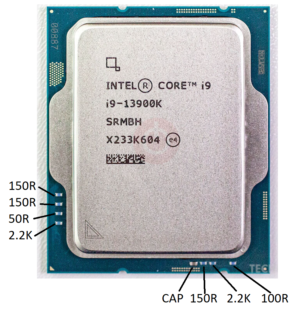
Intel LGA1700 (12th/13th gen, i9 3900k) Top Resistors/Capacitors
If you’re a bit careless with your CPU (especially if e.g., delidding it) you can knock these resistors off the topside. From measuring a known-good device (but without removing them) I measured the following values as a reference:
Danni Build – Feb 11/23
- Hours: 8
- Parts complete: 1 (lateral support), 2 (cylinder support), 3 (frame base)

Start of build. Lots of marking & drilling of items, which was done on a milling machine with DRO. Having the DRO read-out is useful here rather than marking pieces I found. I had mounted cheap iGaging DROs to a small X2 mini-mill, there is a YouTube Video of how I did this. Here is drilling some holes in part 1:
There is a mention in the instructions of making a bushing when making part 3 (frame base) to center it. The instructions say to drill a 7.1mm hole, but that will be too large. Instead measure the actual cross diameter of the piece & drill a hole slightly smaller than this. I used a 3/8 stock drilled with a H bit (G would have been better I think, as I had to clamp it a little ‘too much’):

New England Hardware Security Day 2022 Talk
On April 1st, 2022 I gave a “workshop” at New England Hardware Security Day. This blog post is a quick summary of some of the links to recreate my demos from that talk. Here is a copy of the slides if you’d like them:
DFA on Raspberry Pi with PicoEMP

This demo is pretty simple – it recreates the classic DFA attack on RSA (I find David’s description great here, or you can see my Hardware Hacking Handbook which includes another derivation of it using a different method).
You can see the full code source in my repo from Hackaday Remoticon 2021. That repo just includes the R-Pi Python side (it also makes reference to voltage glitching, which I showed in the talk as another way to perform the demo).
You’ll need to install a specific version of pycryptodome along with a library that performs the analysis afterwards:
pip install pycryptodome==3.1
sudo apt-get install python3-gmpy2
From there you can run rsaglitch.py – if you run it as-is it will sit there waiting for a fault. If you don’t have a FI generator or just want to see it work, simply uncomment the lines that include some example fault output.
The actual fault injection in my demo was done with the PicoEMP. This is a low-cost/open-source EMFI tool. Critically it doesn’t require dangerous exposure to high voltage that some other open-source tools inherently present.
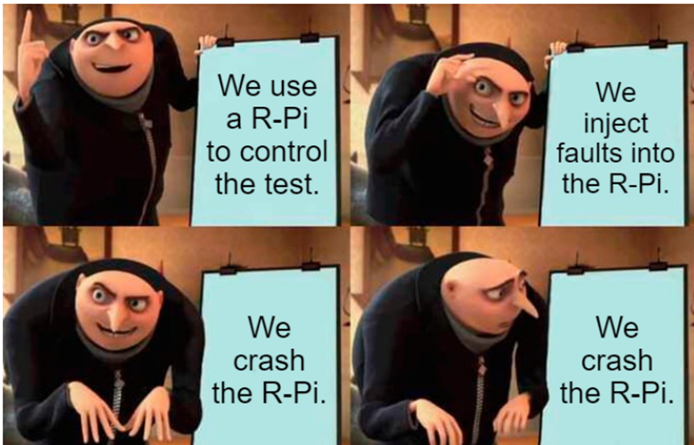
Watch out with this demo – it can be annoying as you crash the R-Pi a lot while dialing it in! And it can take a while to boot, but I gaurantee you it will work!
RISC-V Soft-Core
This demo was based on one of the targets that will come with the ChipWhisperer-Husky, an iCE40 based FPGA target.
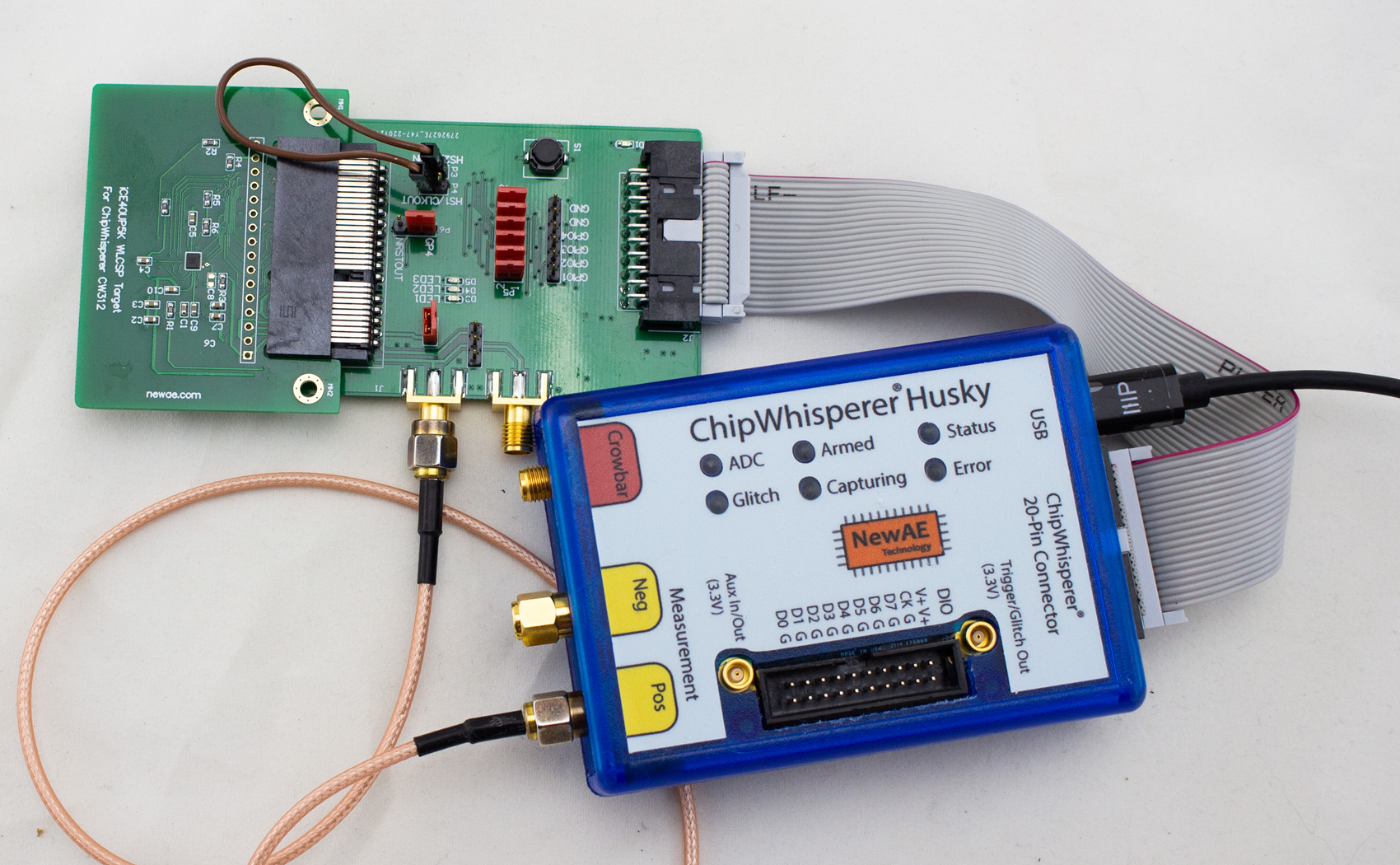
The soft-core in question is the excellent NEORV32 RISC-V core. I find that core’s got great documentation. You don’t need to build the core to use the existing design, as the ChipWhisperer repo has a pre-built binary of the FPGA image. So you can compile software for that image. But it’s fun to build your own core!
- Checkout the neorv32-setups repository.
- Follow instructions to configure the required FPGA toolchain (the ‘osflow’ toolchain).
- Run
make BOARD=iCE40CW312 MinimalBoot
Hardware ECC Attacks
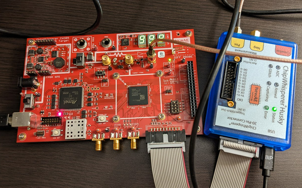
This demo uses the ChipWhisperer CW305 board (here in the A35 variant), which has a series of nice ECC jupyter notebook tutorials . These tutorials will walk you through how the entire attack works:
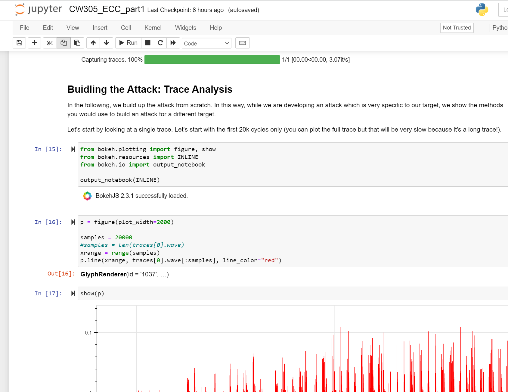
The ECC core is based on the excellent and open-source CrypTech project.
We have a detailed write-up of the attack that can also be helpful to see!
Apple AirTag Teardown & Test Point Mapping
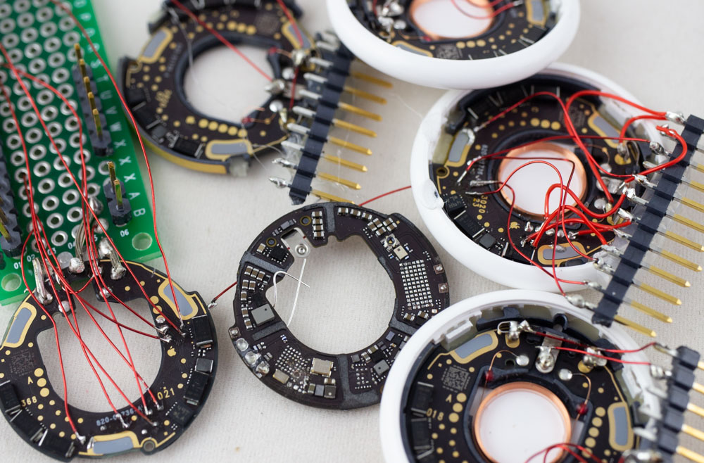
What’s inside of Apple’s new AirTag? There was already an iFixIt teardown (which I swear was missing a few items that are there now), but of course was curious to see what sort of protection was enabled. Notably the nRF chip used is likely vulnerable to a known bypass of security as well. With that in mind, I set out to see how we could dump some data from this thing – the good news is you can access a lot of interesting stuff (including the SPI flash) right from the backside, which requires you to simply pop the first plastic cover off. This is super-easy to do without damaging anything. Going further than that is tricky to keep it all intact.
If you want to jump right to the answers, check out my AirTag-RE repo on github where I list the known test points that will be of interest. You can also see my twitter thread where I started the teardown:
Analog Discover Pro Teardown
NOTE: This was going to be a twitter thread but twitter was down? So this is a lazy blog post…

Anyone used to Digilent would expect this to be based on Zynq or similar – the fact the device has USB + ethernet ports makes it a pretty much sure thing! Taking the screws off the bottom gives us this view:
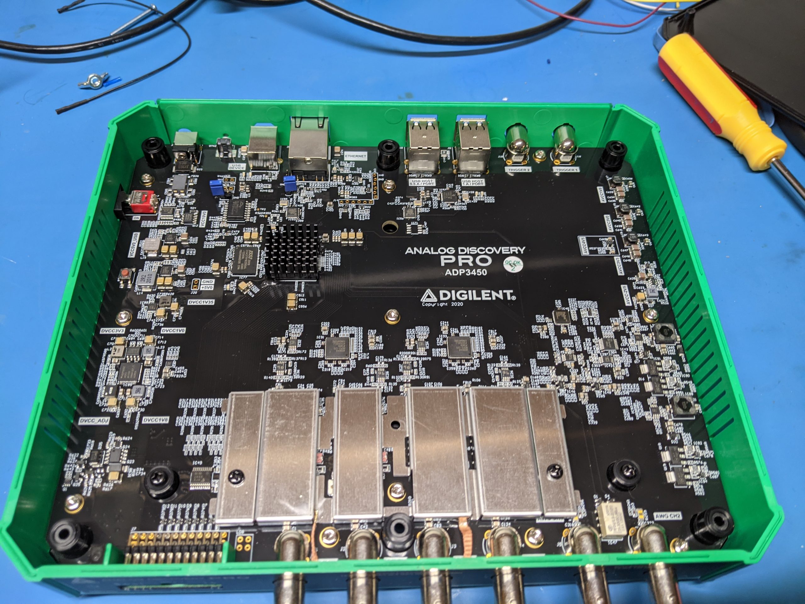
The upper left has a BGA with a heatsink on it – nothing too serious so a small Zynq maybe, or a helper FPGA? The power supplies and similar are all well labeled.
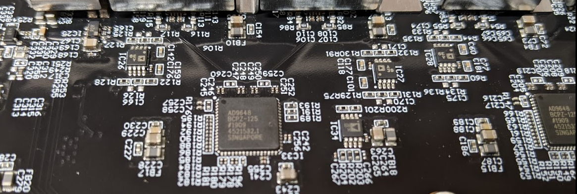
The ADC is a AD9648 – two of them on the 4-channel device. There are a few analog parts you can see, but a lot is hidden behind that metal shield:
Moving the metal shield up reveals it’s mostly just the relays for range switching:

Switching back to digital section, we can see the routing of the Digital IO goes to that BGA part, with DDR memory beside it:
Continue reading Analog Discover Pro TeardownExperimenting with Metastability and Multiple Clocks on FPGAs
NOTE: This article appeared in Issue 293 of Circuit Cellar, back in December 2014. I’ve posted it here for your reading pleasure as well. References to previous articles are for Circuit Cellar Issues, as this was originally written for the print publication. This version differs slightly from the print version – this is my own ‘author copy’ version before the Circuit Cellar editing. References to “ProgrammableLogicInPractice.com” are broken for now, but material has been mirrored to the bottom of this page.
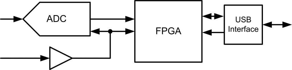
One of the most critical aspects of any FPGA design is where two clock domains meet. The general rule is to avoid this at all costs, but there are situations where it’s unavoidable. A simple situation is shown in Fig. 1, where our system is receiving data from an ADC, but speaking on a common bus. The ADC sample rate is generated from an external source, and might change for specific applications.
BAM BAM!! On Reliability of EMFI for in-situ Automotive ECU Attacks
This post is a summary of some work on an accepted paper for ESCAR EU 2020. This work was demonstration on certain NXP chips & GM ECUs, but the idea of both the attack & understanding how portable results are is applicable across the entire domain.
NOTE TO CAR TUNERS: I won’t perform this for hire on your ECU, please don’t email me asking this. The cost for me to do this type of work under hire would also be many times the HPTuners fee, and without any of of the actual tuning interface (I’m only attacking the bootloader, I never ever built a reflash tool that would be needed, yet alone the mapping work etc).
You can find links to:
🔧 The full technical paper in PDF
🔧 The talk slides in PDF
🔧 YouTube “video log” during work: Part 1, Part 2, Part 3, Part 4
This work was presented as a way to help automotive system designers understand the “real” threat to their systems, something that is hard to do when tuners hide their methods for commercial reasons. While I don’t know if the method I’m presenting is used by the car tuners, I assume some variant of it has been before (I doubt I’m the “true” discoverer). As I mentioned in the paper, I’m also not the first to turn EMFI onto automotive devices in an academic setting (another nice paper ref’d is the Safety != Security work). One contribution of my work is it directly talks about practicality, something critical for threat modelling but often skipped due to how messy this is. You can build the attack into a “portable rig” as shown here in a final demonstration:
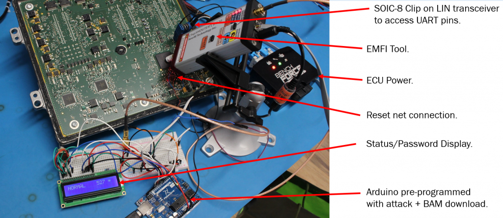
This portable rig is designed to show something along the lines of “pro garage” or “tuner garage” capabilities. It doesn’t need a ton of expertise to execute the attack, and opening up ECUs and probing them is widely done as part of regular tuning already (often called a type of “bench flash”). The real research wasn’t done with the Arduino setup, but instead using ChipWhisperer as part of the triggering with Python scripts searching:

The Arduino demonstration shown previously is not usable as-is for tuning. It’s very fiddly and hasn’t been optimized, so I can’t productize what was shown there easily (you can tell I get sick of people looking for tuning solutions…).
The attack is possible on these devices, as they have a hardware bootloader enabled with some pin on the board. This requires you to short that pin to GND to enter the bootloader mode, at which point the device is looking for a password. Using electromagnetic fault injection, you can bypass the password check such that an incorrect password is accepted.
You can use power analysis to discover some of the timing, as done in the paper. Comparing a good password to a bad password shows a clear point in time where the password logic differs:
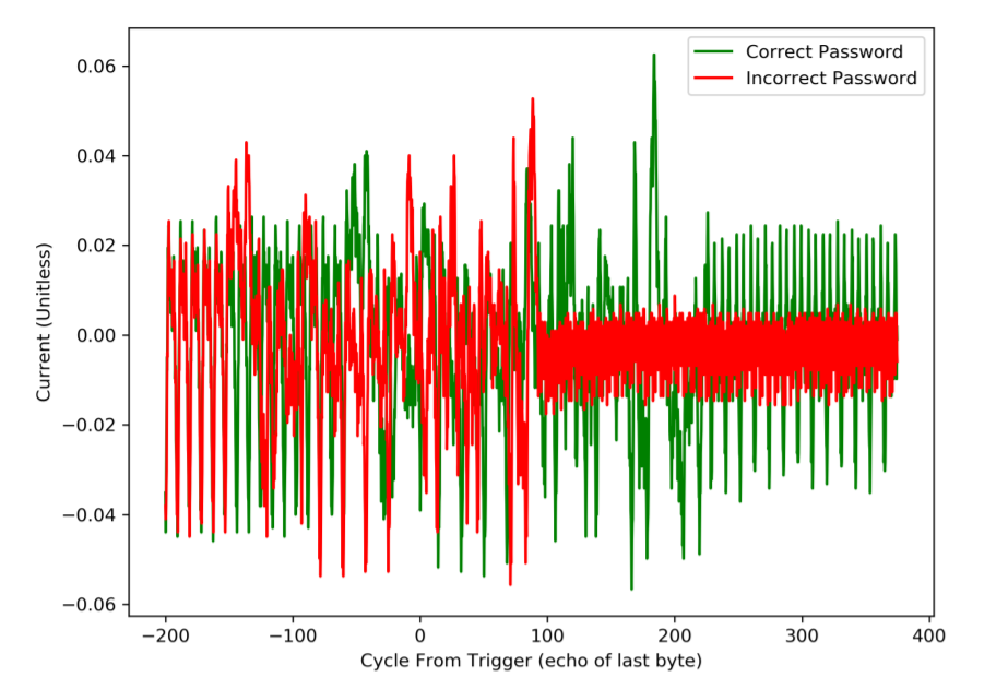
Interestingly, you can also see the red “incorrect password” trace appears to spin into an infinite loop (or similar), which would be around cycle 100 on the above figure.
As an important caveat: EMFI works against almost any microcontroller. Thus there is no “flaw” in the NXP MCU or GM usage of it, many other devices can be attacked using this same technique. The NXP MCU has long-term support (meaning it sticks around 15+ years), and was designed long before fault injection was on the radar of these devices as a realistic threat.
See the full paper for more details of the work.
FPGA Board Design Tips
NOTE: This article appeared in Issue 315 of Circuit Cellar, back in October 2016. I’ve posted it here for your reading pleasure as well. References to previous articles are for Circuit Cellar Issues, as this was originally written for the print publication. This version differs slightly from the print version – this is my own ‘author copy’ version before the Circuit Cellar editing.
Back in December 2015, I discussed how I solder BGA devices (such as FPGAs) using a low-cost reflow oven. This article will discuss the design of the FPGA board itself, which you could then assemble using the tips in my previous article.
I’ll assume you have a rough idea of what external parts you need, as they will be highly dependant on what you are trying to accomplish with your design. In addition to design-specific information, there are a few standards external requirements such as programming interface, communications, and power. This article will briefly cover some of these external requirements, but the concentration of this article is how to physically lay-out the FPGA board at a reasonable cost.
Some of the topics I covered previously too – for example in my June 2015 article I discussed the use of a generic USB microcontroller as a FPGA interface chip, which is very useful if you need to shuffle data to/from the FPGA.
So let’s assume you have a (mostly) complete schematic, and are wondering how to make this a reality. Let’s start with setting a target goal in terms of board requirements.
PCB Specifications
Assuming this design will be either a prototype run or possibly a small production run, it makes sense to design your PCB with specific requirements in mind to keep costs reasonable. The two PCB specifications you are most commonly told are the minimum “trace/space” (that is, minimum width of a trace, and minimum spacing between copper features), and the minimum drill size.
As I mentioned in my previous article, I’m often using an overseas PCB fab at 3pcb.com, although many other options are worth trying. They offer a variety of trace/space and drill size options, so I’ll target a 5 mil space/trace with 0.2 mm drill. This is a fairly “standard” technology option, so shouldn’t be a problem when moving towards a small production run (i.e., Qty 100-200).
To give you an idea of what we’re working with, Figure 1 shows an example of the final PCB I designed and assembled. This uses a Spartan 6 LX45 FPGA with an Atmel SAM3U microcontroller for high-speed USB communications.